GTU COA (Computer Organization & Architecture) Summer 2022 Paper Solutions
Download Question Paper : click here
Q.1
(a) What is binary and decimal equivalent of F8 hexadecimal value?
Binary equivalent of F8 -
First let’s convert F to binary. We know F = 15 (in hexadecimal).
So 15 (hexadecimal) can be represented by: 1111 in binary
& binary equivalent of 8: 1000
Therefore, F8 = 1111 1000
Decimal Equivalent of F8 -
(F8)₁₆ = (15 × 16¹) + (8 × 16⁰) = (248)₁₀
(b) Write Steps for two n digit numbers subtraction in base r
- Add the minuend M to the r's complement of the subtrahend N to perform:
- If M≥ N, the sum will produce an end carry, which is discarded. what is left is the result, M - N
- If M < N, the sum does not produce and end carry and is equal to , which is the r’s complement of ( N-M). To obtain the answer in a familiar form, take the r’s complement of the sum and place a negative sign in front.
- Obtain the final result: To obtain the result in a familiar form, take the r's complement of the sum calculated in the previous step and place a negative sign in front. This ensures that the result is represented as a negative number when M is less than N.
Example :

Example :

(c) List and explain Memory reference instructions in detail.
A memory reference instruction, is a type of instruction that involves accessing or manipulating data stored in memory. These instructions are commonly used to read data from memory (load) or write data to memory (store).
We have 7 different types of Memory reference instructions
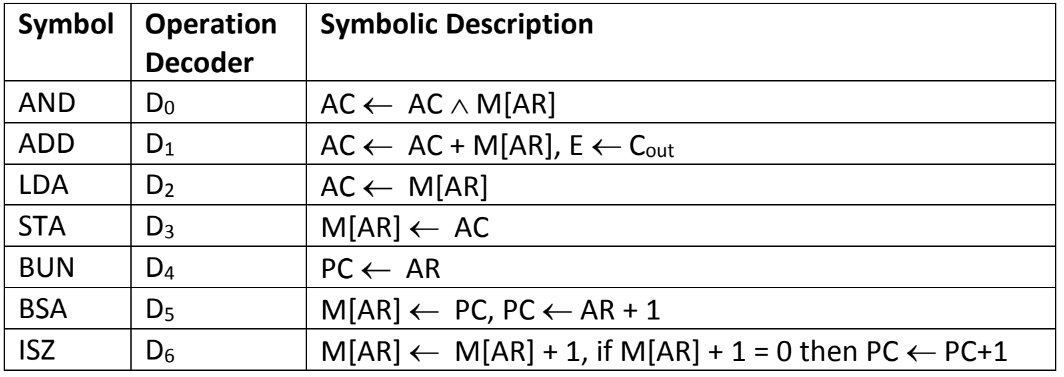
AND to AC
This is an instruction that performs the AND logic operation on content of accumulator and the operand stored into the memory specified by the address register. The result of the operation is transferred to AC (accumulator).
D0T4: DR←M[AR]
D0T5: AC ← AC ^ DR, SC ← 0
ADD to AC
Performs the Addition of accumulator and the data stored in memory and the result is stored back into the accumulator. If carry is generated in this operation, it gets stored in E (extended accumulator) flip flop
D1T4: DR ← M[AR]
D1T5: AC ← AC + DR, E ← Cout, SC ← 0
LDA: Load to AC
This instruction transfers the memory word specified by the effective address to AC. In simple terms, it transfers data stored in memory to accumulator.
D2T4: DR ← M[AR] D2T5: AC ← DR, SC ← 0
STA: Store AC
Store the content of AC (accumulator) to the memory word specified by the address register
D3T4: M[AR] ← AC, SC ← 0
BUN: Branch Unconditionally
This instruction transfers the program to instruction specified by the effective address. The BUN instruction allows the programmer to specify an instruction out of sequence and the program branches (or jumps) unconditionally.
D4T4: PC ← AR, SC ← 0
BSA: Branch and Save Return Address
This instruction is useful for branching to a portion of the program called a subroutine or procedure. When executed, the BSA instruction stores the address of the next instruction in sequence (which is available in PC) into a memory location specified by the effective address.
M[AR] ← PC, PC ← AR + 1 M[135] ← 21, PC ←135 + 1 = 136
ISZ: Increment and Skip if Zero
Increment the data stored in memory specified by the address register by 1 and if it is zero after incrementing, then skip the next instruction. Incremented content needs to be stored back into memory.
D6T4: DR ← M[AR] D6T5: DR ← DR + 1 D6T4: M[AR] ← DR, if (DR = 0) then (PC ← PC + 1), SC ← 0
Q.2
(a) What is arithmetic micro operation?
- Arithmetic microoperations are microoperations that perform arithmetic operations on numeric data stored in register.
- The basic arithmetic micro-operations are:
- Addition
- Subtraction
- Increment
- Decrement
- Shift
- The additional arithmetic micro operations are:
- Add with carry
- Subtract with borrow
- Transfer/Load , etc.
(b) What is RAM and ROM?
- RAM and ROM are two types of computer memory used to store data and instructions.
RAM (Random Access Memory):
- Volatile Memory: RAM is a type of computer memory that is volatile, meaning its contents are temporary and are lost when the power is turned off or interrupted.
- Main Memory: RAM serves as the primary working memory of a computer system. It stores data that is actively being used by the CPU and running programs.
- Random Access: RAM is called "random access" because the CPU can directly access any memory location in RAM in constant time, regardless of the location's physical proximity.
ROM (Read-Only Memory):
- Non-Volatile Memory: ROM is a type of computer memory that is non-volatile, meaning its contents are permanently stored and retained even when the power is turned off.
- Pre-Programmed Data: ROM contains data that is programmed during manufacturing and cannot be modified or erased by normal computer operations.
- Firmware and Boot Instructions: ROM is commonly used to store firmware, which contains low-level software instructions and settings for devices such as BIOS in a computer.
(c) Draw and explain working of 4 bit binary adder.
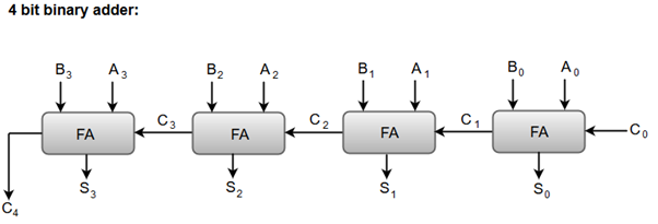
- Inputs: The 4-bit binary adder takes two 4-bit binary numbers, A and B, as input. These numbers are represented using four binary digits, or bits (A3A2A1A0 and B3B2B1B0).
- Full Adder: Each bit addition is performed by a full adder circuit. In a 4-bit binary adder, there are four full adders connected.
- Bit-wise Addition: Starting from the rightmost bit (the least significant bit), each pair of corresponding bits (A0 and B0, A1 and B1, A2 and B2, A3 and B3) are added using the full adder circuit.
- Inputs to Full Adder: Each full adder takes three inputs:
- The two bits being added (A_i and B_i, where i represents the bit position, ranging from 0 to 3).
- A carry-in from the previous lower-order bit.
- Outputs of Full Adder: Each full adder produces two outputs:
- The sum of the inputs A_i, B_i, and C_i-1, which represents the ith bit of the result.
- A carry-out (C_i) that is propagated to the next higher-order bit.
- Carry Propagation: The carry-out (C_i) from each full adder is connected as the carry-in (C_i-1) to the next higher-order full adder. This carries the carry-over from the addition of the current bit pair to the next bit pair.
- Sum and Carry Outputs: The final outputs of the 4-bit binary adder are:
- The four-bit sum (S3S2S1S0), where each bit represents the result of the addition of the corresponding bits (A_i and B_i).
- The carry-out (C4), which represents the carry-over from the addition of the most significant bit pair (A3 and B3).
OR
(c) State and Explain any seven logic micro operation.
Logic micro operations specify binary operations for strings of bits stored in registers.
These operations consider each bit of the register separately and treat them as binary variables.
Clear
A clear microoperation is a logic operation that sets the value of a register or memory location to zero or a predefined state, effectively clearing its contents.
Microoperation: F←0
AND
The AND logic microoperation takes two bits as input and produces an output bit. It results in 1 (true) only when both input bits are 1; otherwise, the output is 0 (false).
Microoperation: F←A ∧ B
Transfer A
The transfer logic microoperation simply copies the value of one bit or group of bits from a source to a destination without any modification.
Microoperation: F←A
Exclusive OR
The exclusive OR (XOR) logic microoperation takes two bits as input and produces an output bit. It results in 1 (true) when the two input bits are different (one is 0 and the other is 1), and 0 (false) when the input bits are the same (both 0 or both 1).
Microoperation: F←A⊕B
OR
The OR logic microoperation takes two bits as input and produces an output bit. It results in 1 (true) if at least one of the input bits is 1, and 0 (false) only if both input bits are 0.
Microoperation: F←A∨B
NOR
The NOR logic microoperation takes two bits as input and produces an output bit. It results in 1 (true) only when both input bits are 0, and 0 (false) otherwise.
Microoperation: F←(A∨B)’
Complement A
The complement A logic microoperation, also known as the NOT operation, takes a single bit as input and produces the opposite value as output. It reverses the input bit, changing 1 (true) to 0 (false) and 0 (false) to 1 (true).
Microoperation: F←A̅
Q.3
(a) List out Register for basic computer.
- Address Register (AR)
- Program Counter (PC)
- Data Register (DR)
- Accumulator (AC)
- Input Register (INPR)
- Instruction Register (IR)
- Temporary Register (TR)
- Output Register (OUTR)
(b) Explain register reference instruction format.
A register reference instruction is a type of instruction that involves accessing or manipulating data stored in a register.
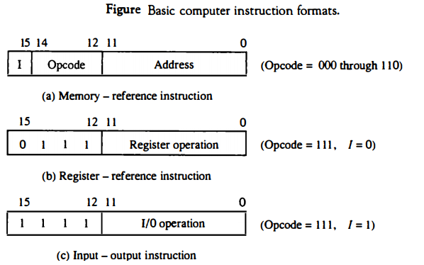
Fig. (b) shows register reference instruction format
The register reference instruction format typically consists of three main blocks:
- Addressing Block (15th bit): This block specifies the addressing mode used in the instruction. In the case of a register reference instruction, this block is often fixed to a value of 0 since the instruction operates directly on registers.
- Opcode Block (12-14): This block holds the opcode, which determines the specific operation to be performed by the instruction. The opcode indicates whether the instruction is a load, store, arithmetic operation, or logical operation. In the case of a register reference instruction, this block is often fixed to a value of 111.
- Register Operation Block (0-11): This block specifies the registers involved in the instruction. It identifies the source and destination registers, or any other registers needed for the operation. The registers are typically represented by their names or numbers.
(c) Explain register transfer using block diagram and timing diagram.
Register transfer refers to the movement of data between registers in a computer system. It involves transferring binary data from one register to another, loading data into a register, or storing data from a register into memory.
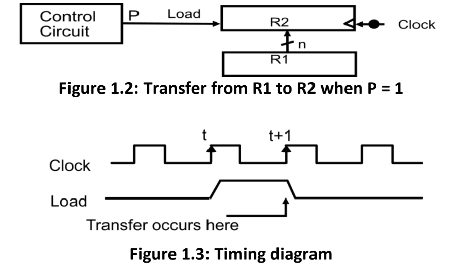
- Control Circuit: The control circuit generates control signals that coordinate and control the transfer of data between registers. It generates signals such as load, enable, or clock signals based on the instruction being executed.
- R1 and R2: R1 and R2 represent two registers involved in the register transfer operation. These registers store binary data.
- Clock: The clock signal is a periodic signal that synchronizes the operation of the entire system. It ensures that the register transfer occurs at the correct time and in a coordinated manner.
- At t+1, only when the signal is going low, the transfer of data will occur.
The process of register transfer involves selecting the source register, activating the necessary control signals, and transferring the data to the destination register. It can also involve performing computations or transformations on the data during the transfer. Register transfer operations are essential for executing instructions, manipulating data, and enabling communication between various components of a computer system.
Register transfer operations are governed by control signals, which are generated by a control unit based on the instructions being executed. These control signals coordinate the timing and sequencing of the register transfer process, ensuring that data is moved accurately and efficiently.
OR
Q.3
(a) Draw and explain control unit diagram for basic computer.
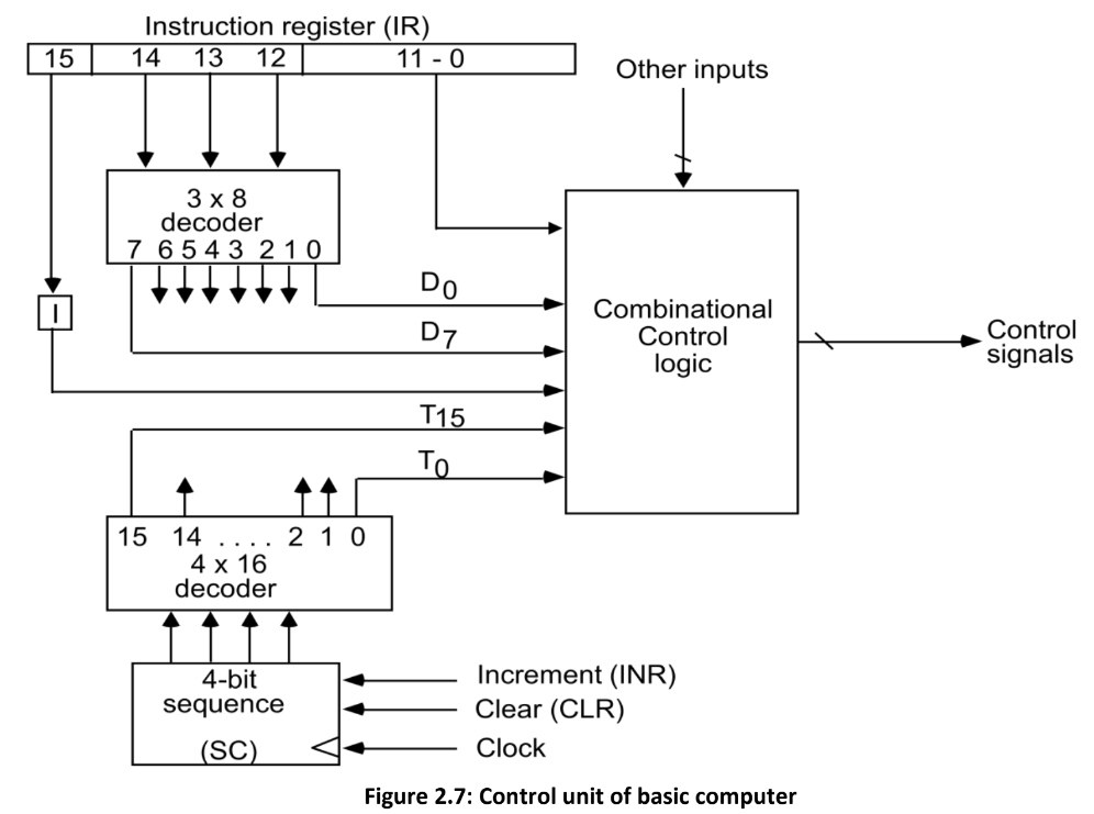
The CPU control unit is a component of the computer’s CPU (central processing unit) that directs the processor’s operation. The control unit’s job is to instruct the computer’s arithmetic/logic unit, memory, and input and output devices on how to respond to the instructions supplied to the processor.
A control unit receives data from the user and translates it into control signals that are subsequently delivered to the central processor.
Components of the Control Unit:
- Two Decoders: Decoders receive input signals and generate output signals based on the specific combination of inputs, helping to decode instruction codes and generate control signals.
- Sequence Counter: The sequence counter keeps track of the current and next instructions to be executed, maintaining the program flow by incrementing the instruction address and ensuring instructions are executed in the correct order.
- Control Logic Gates: Control logic gates manipulate control signals using logical operations to activate or deactivate specific components of the computer system based on the requirements of the executing instruction.
(b) State various phases of instruction cycle.
The instruction cycle is a process of fetching, interpreting, and executing instructions in a computer. It consists of the following phases:
Fetch Instruction: The processor fetches the next instruction from memory using the program counter (PC) to determine the address, loading it into an instruction register for further processing.
T0: AR ← PC
T1: IR ← M[AR], PC ← PC + 1
Decode the Instruction: The fetched instruction is decoded to determine the type of instruction, its operation and operand(s), extracting the necessary information for the subsequent steps.
T2: D0,…,D7 ← Decode IR (12-14), AR ←IR (0-11), I ← IR (15)
If D7 = 1 then instruction must be register reference or Input-Output else memory reference instruction.
- Read Effective Address: If the instruction has an indirect address, this phase involves accessing memory to fetch the actual address or data required for the instruction's execution.
- Execute the Instruction: The instruction is executed by performing the specific operation indicated by the decoded instruction, which may involve arithmetic, logical, or control operations based on the instruction type and operands.
(c) Explain any four input output reference instruction.
- Input/output (I/O) instructions are specific instructions in computer architecture that facilitate the transfer of data between the CPU and external devices, such as keyboards, displays, disks, or networks etc.
- Input-output instructions have an operation code 1111 and are recognized by the control when D7 = 1 and I = 1.
- The remaining bits of the instruction specify the particular operation.
Four I/O instructions:
- INP
The INP instruction transfers the input information from INPR into the eight low-order bits of AC and also clears the input flag to 0.
AC(0-7) ← INPR, FGI ← 0
- OUT
The OUT instruction transfers the eight least significant bits (last 8 bits) of AC into the output register OUTR and clears the output flag to 0.
OUTR ← AC(0-7), FGO ← 0
- SKI & SKO
These two instructions check the status of the flags and cause a skip of the next instruction if the flag is 1.
if(FGI = 1) then (PC PC + 1) - Skip on input flag
if(FGO = 1) then (PC PC + 1) - Skip on output flag
- ION
Interrupt Enable ON refers to activation or enabling of interrupts in a computer system. Enabling interrupts allows the CPU to respond to interrupt requests from external devices or software events.
IEN ← 1
Q.4
(a) Draw flowchart of first pass assembler.

(b) Write assembly language program to add two numbers.
| Memory Address | Instruction | RTL Expression | Comment |
|---|---|---|---|
| 2000 | LDA 2050 | A <- [2050] | Load the first 8-bit number from memory into the accumulator (A) register. |
| 2003 | MOV H, A | H <- A | Copy the value from the accumulator (A) register to the H register. |
| 2004 | LDA 2051 | A <- [2051] | Load the second 8-bit number from memory into the accumulator (A) register. |
| 2007 | ADD H | A <- A + H | Add the value in the H register to the value in the accumulator (A) register. |
| 200D | SHLD 3050 | [3051] <- A, [3050] <- H | Store the result in memory. |
| 2010 | HLT | Halt | Halt the program. |
(c) Write assembly language program to multiply two numbers.
| Memory Address | Instruction | RTL Expression | Comment |
|---|---|---|---|
| 2000 | LDA 2050 | A <- [2050] | Load the first number from memory into A |
| 2003 | MOV B, A | B <- A | Copy the value from A to B |
| 2004 | LDA 2051 | A <- [2051] | Load the second number from memory into A |
| 2007 | MUL B | A <- A * B | Multiply the contents of A and B |
| 2008 | STA 3050 | [3050] <- A | Store the result in memory |
| 200B | HLT | Halt | Halt the program |
- Load the first number from memory into A (LDA 2050): The program retrieves the first number, also known as the multiplicand, from memory and stores it in register A.
- Copy the value from A to B (MOV B, A): The value in register A, representing the multiplicand, is copied to register B for further processing.
- Load the second number from memory into A (LDA 2051): The program retrieves the second number, also known as the multiplier, from memory and stores it in register A.
- Multiply the contents of A and B (MUL B): The program performs the multiplication operation by multiplying the values in registers A and B, which represent the multiplier and multiplicand, respectively.
- Store the result in memory (STA 3050): The resulting product is stored in memory at the specified location.
- Halt the program (HLT): The program execution is halted/stopped, indicating the completion of the multiplication operation.
These steps outline the process of multiplying two numbers using the provided assembly language program
OR
Q.4
(a) What is address sequencing?
- Address sequencing refers to the process of determining the sequence in which memory addresses are accessed or executed during the execution of a program or instruction.
- Control Address Register (CAR) Incrementing: The control address register is responsible for storing the address of the next instruction to be fetched from control memory. During address sequencing, the CAR is incremented to point to the next instruction in the sequence.
- Branching: Address sequencing involves branching based on certain conditions. This can be an unconditional branch, where the control address register is directly updated to a specific address, or a conditional branch, where the branching is determined by the status bit conditions.
- Mapping Process: The address sequencing process also includes a mapping process to determine the specific address within the control memory. This mapping is typically done by using specific bits of the instruction address to identify the correct location in control memory where the instruction is stored.
- Subroutine Return: Address sequencing provides a facility for subroutine return. When a subroutine is called and its execution is complete, the address sequencing mechanism allows for the return to the calling program by updating the control address register with the address to resume execution after the subroutine.
(b) Write assembly language program to subtract one number from other number.
| Memory Address | Instruction | Comment |
|---|---|---|
| 2000 | LDA 2050 | Load the first number from memory into A |
| 2003 | MOV B, A | Copy the value from A to B |
| 2004 | LDA 2051 | Load the second number from memory into A |
| 2007 | SUB B | Subtract the contents of B from A |
| 2008 | STA 3050 | Store the result in memory |
| 200B | HLT | Halt the program |
(c) Explain booth’s multiplication algorithm with example.
Booth algorithm gives a procedure for multiplying binary integers in signed- 2’s complement representation
- Booth's algorithm reduces the number of partial products, resulting in fewer additions or subtractions.
- It utilizes shifting operations for quick multiplication by powers of 2 and aligning partial products.
- The algorithm is particularly efficient when the multiplier has consecutive zero bits, minimizing required operations.
It works on the string bits 0's in the multiplier that requires no additional bit only shift the right-most string bits and a string of 1's in a multiplier bit weight 2ᵏ to weight 2ᵐ that can be considered as 2ᵏ⁺¹ - 2ᵐ
Example - Let’s multiply the two numbers 7 and 3 by using the Booth's multiplication algorithm.
Here we have two numbers, 7 and 3. First of all, we need to convert 7 and 3 into binary numbers like 7 = (0111) and 3 = (0011). Now set 7 (in binary 0111) as multiplicand (M) and 3 (in binary 0011) as a multiplier (Q). And SC (Sequence Count) represents the number of bits, and here we have 4 bits, so set the SC = 4. Also, it shows the number of iteration cycles of the booth's algorithms and then cycles run SC = SC - 1 time.
| Qₙ | Qₙ₊₁ | M = (0111) M' + 1 = (1001) & Operation | AC | Q | Qₙ₊₁ | SC |
|---|---|---|---|---|---|---|
| 1 | 0 | Initial | 0000 | 0011 | 0 | 4 |
| Subtract (M' + 1) | 1001 | |||||
| 1001 | ||||||
| Perform Arithmetic Right Shift operations (ashr) | 1100 | 1001 | 1 | 3 | ||
| 1 | 1 | Perform Arithmetic Right Shift operations (ashr) | 1110 | 0100 | 1 | 2 |
| 0 | 1 | Addition (A + M) | 0111 | |||
| 0101 | 0100 | |||||
| Perform Arithmetic right shift operation | 0010 | 1010 | 0 | 1 | ||
| 0 | 0 | Perform Arithmetic right shift operation | 0001 | 0101 | 0 | 0 |
The numerical example of the Booth's Multiplication Algorithm is 7 x 3 = 21 and the binary representation of 21 is 10101. Here, we get the resultant in binary 00010101. Now we convert it into decimal, as (000010101) = 2*4 + 2*3 + 2*2 + 2*1 + 2*0 => 21
Q.5
(a) Explain register stack.
- Register stack is a storage mechanism that follows the Last-In-First-Out (LIFO) principle.
- It has a fixed number of registers, usually fewer than general-purpose registers.
- The primary operations are push (addition) and pop (removal) of data.
- It uses a stack pointer to keep track of the top position of the stack.
- Register stack provides quick and direct access to the topmost register.
(b) What is difference between two address and three address instructions?
Two-Address Instructions:
- Two-address instructions involve operations with two operands: one source and one destination.
- The result of the operation is stored directly in the destination operand, overwriting its previous value.
- The two operands can be memory locations, registers, or a combination of both.
- Example: ADD A, B - Adds the value of operand B to the value in register A and stores the result in register A.
Three-Address Instructions:
- Three-address instructions involve operations with three operands: two sources and one destination.
- The result of the operation is stored in the destination operand without affecting the source operands.
- The three operands can be memory locations, registers, or a combination of both.
- Example: MUL C, A, B - Multiplies the values of operands A and B and stores the result in operand C without modifying A or B.
(c) Write a note on asynchronous data transfer.
Asynchronous data transfer refers to the process of transferring data between two independent units or devices where the internal timing of each unit is independent of the other.
There are two ways of achieving it -
Strobe control and Handshaking
Strobe control -
This method employs a single control line to time each transfer. This control line is also known as a strobe, and it may be achieved either by source or destination, depending on which initiate the transfer.
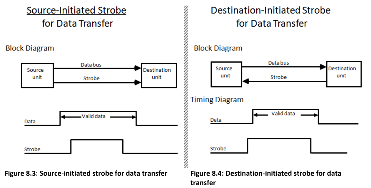
Source-initiated strobe for data transfer
- In the source-initiated strobe method, the source unit activates a strobe pulse to indicate that valid data is available on the data bus.
- The destination unit responds to the strobe signal and retrieves the data from the bus, typically during the active duration of the strobe signal.
Destination-initiated strobe for data transfer
- In the destination-initiated strobe method, the destination unit activates a strobe pulse to request data transfer from the source unit.
- Upon receiving the strobe signal, the source unit places the requested data onto the data bus.
- The destination unit retrieves the data from the bus during the active duration of the strobe signal.
Handshaking -
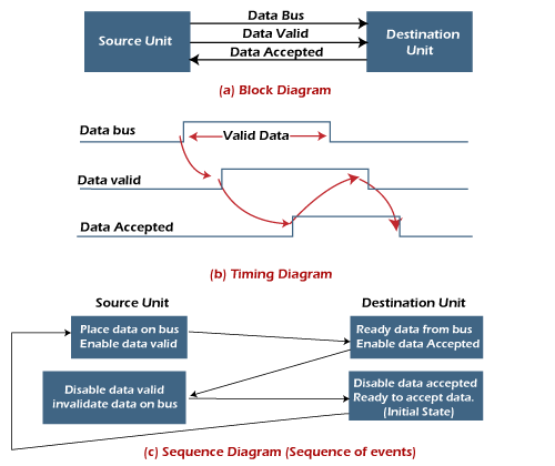
The handshake method solves the problem of Strobe method by introducing a second control signal that provides a reply to the unit that initiates the transfer.
Source-initiated transfer using handshaking
- In source-initiated transfer using handshaking, the source unit controls the timing of data transfer by initiating the handshaking signals, while the destination unit responds to the signals to indicate its readiness to receive the data.
Destination-initiated transfer using handshaking
- In destination-initiated transfer using handshaking, the destination unit initiates the data transfer by requesting data from the source unit using handshaking signals, and the source unit responds to indicate its readiness to transmit the data.
OR
Q.5
(a) What is difference between direct and indirect addressing mode?
- In direct addressing mode (I = 0), the instruction directly specifies the operand, indicating exactly which data to use.
- In indirect addressing mode (I = 1), the instruction specifies the memory address where the operand is stored, and the computer looks in that memory location to find the actual data to use.
- Direct addressing provides a straightforward way to access specific data, while indirect addressing allows for more flexibility by using memory addresses to access the desired data.
(b) Explain arithmetic pipeline.
Arithmetic pipeline is a technique used to enhance the performance of arithmetic operations by breaking them down into smaller stages or sub-operations.
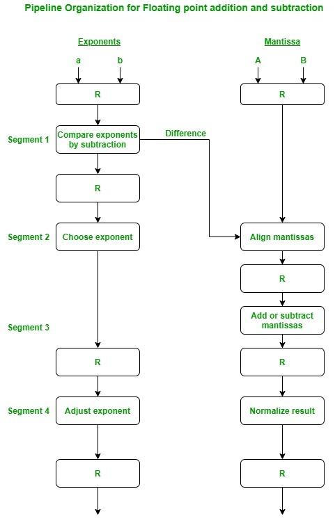
Floating point addition using arithmetic pipeline :
The following sub operations are performed in this case:
- Compare the exponents: In this stage, the exponents of the operands are compared to determine the necessary alignment and scaling for further calculations.
- Align the mantissas: This stage adjusts the position of the mantissas so that they have the same exponent, allowing for proper addition, subtraction, or other arithmetic operations.
- Add or subtract the mantissas: The mantissas are added or subtracted based on the desired arithmetic operation, considering any carry or borrow from the previous stage.
- Normalize the result: The result is normalized by adjusting the exponent and mantissa to ensure proper representation, eliminating any leading or trailing zeros and maintaining accuracy.
(c) Write a short note on virtual memory.
Virtual memory is a memory management technique used that allows the system to use more memory than physically available. It provides a level of abstraction between the logical memory seen by the programs and the physical memory modules installed in the computer.
- Virtual memory provides a larger address space to programs than the physical memory by using a combination of RAM and disk storage.
- It allows the system to store parts of the running programs in the disk, called the swap space, while keeping the frequently accessed portions in RAM.
- When a program needs to access data that is not currently in RAM, a process called paging occurs, where the required page is fetched from disk to RAM.
- Virtual memory enables efficient memory allocation, as it allows multiple programs to run simultaneously without the need for the entire program to be loaded in memory.
- Virtual memory supports the concept of address spaces, which provide a logical view of memory for each process, allowing them to operate independently of each other.
- It plays a crucial role in memory management by dynamically allocating and deallocating memory pages as needed, optimizing resource usage.
- It provides benefits like memory protection, as each program is isolated and cannot access the memory allocated to other programs, ensuring system stability and security.
Virtual memory enhances the system's performance by providing the illusion of a larger memory space and optimizing memory allocation based on the demands of running programs.