GTU COA (Computer Organization & Architecture) Winter 2022 Paper Solutions
Download Question Paper : click here
Q.1
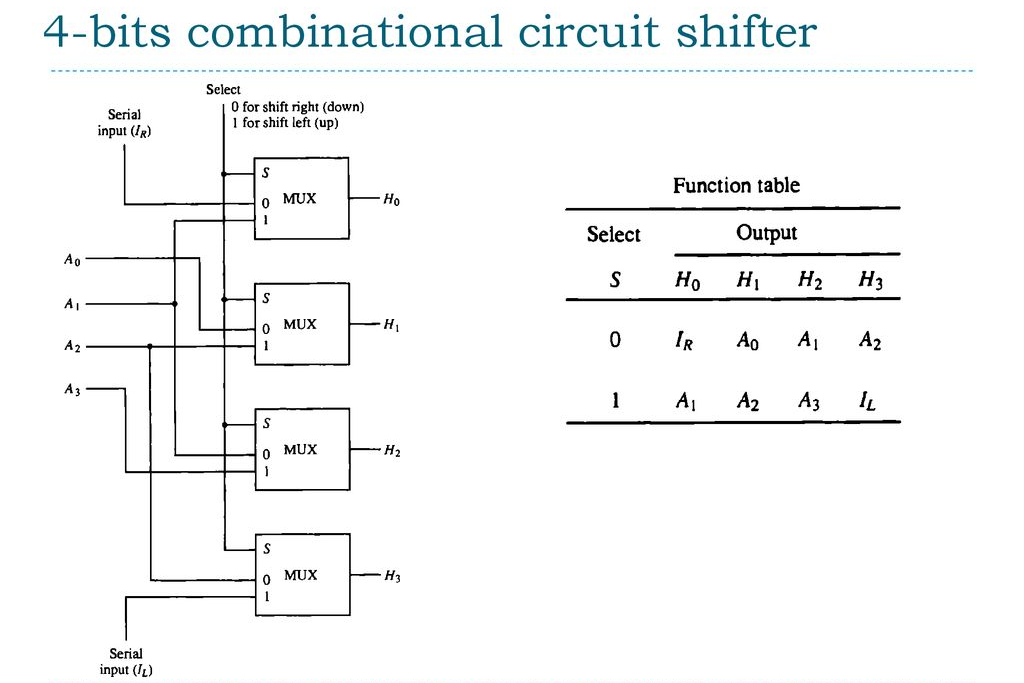
(a) Draw the block diagram of 4-bit combinational circuit shifter.
(b) Construct diagram of common bus system of four 4-bits registers with diagram.
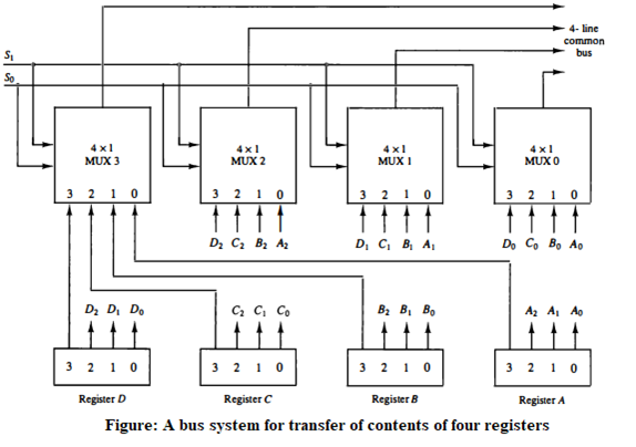
- A typical digital computer has many registers, and paths must be provided to transfer information from one register to another. The number of wires will be excessive if separate lines are provided for each register, More efficient system would be common bus system to transfer information between registers.
- A bus structure consists of a set of common lines, one for each bit of a register, through which binary information is transferred one at a time.
- Control signals/Selection Lines determine which register is selected by the bus during each particular register transfer.
- One way of constructing a common bus system is with multiplexers.
- In this system, four 4-bit registers (A, B, C, and D) share a common bus.
- The bus allows each register to communicate with other registers and external devices.
- Each register has an input and output port connected to the bus.
- When a register needs to read or write data, it sends a request to the bus controller, which then grants access to the bus.
- The bus controller also ensures that only one register can write to the bus at a time to avoid data collisions
(c) What is the role of sequence counter(SC) in control unit? Interpret its concept with the help of its three inputs using diagram.
The sequence counter is a specialized register within the control unit that keeps track of the current microinstruction being executed in the instruction cycle.
Diagram -
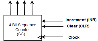
- Increment: This input signal is responsible for incrementing the value of the SC. When activated, it causes the SC to move to the next state or count up by one. It enables sequential progression through the microinstructions stored in the control memory.
- Clear: The clear input signal is used to reset the SC to a specific starting state. When activated, it clears the current value of the SC and sets it to the initial state. This input is typically used during initialization or to restart the sequence from the beginning.
- Clock: The clock input signal provides the timing for the SC. It determines the rate at which the SC advances from one state to the next. On each clock pulse, the SC evaluates its inputs and updates its state accordingly. The clock input ensures synchronous operation and proper synchronization of the SC with other components of the computer system.
Role of sequence counter -
- Instruction sequencing: The sequence counter controls the flow of microinstructions during the execution of an instruction. It determines the order in which microinstructions are fetched, decoded, and executed.
- Incrementing: The sequence counter is typically incremented after each microinstruction execution, causing it to point to the next microinstruction in the sequence. This enables the control unit to fetch and execute the next microinstruction in the instruction cycle.
- Branching and looping: The sequence counter allows for branching and looping within the instruction sequence. It can be modified to jump to a different address or loop back to a previous address, altering the execution flow based on certain conditions or instructions.
- Synchronization: The sequence counter ensures proper synchronization between the control unit and other components of the computer system. It helps coordinate the timing and sequencing of operations, ensuring that the correct microinstructions are executed in the right order.
So the sequence counter is responsible for maintaining the correct order of microinstruction execution, enabling the control unit to properly interpret and execute instructions. It provides the necessary control and coordination for the effective operation of the computer system.
Q.2
(a) List out names of eight main registers of basic computer with their symbolic name and purpose.
Here are the eight main registers of a basic computer with their symbolic name and purpose:
- Data Register (DR) : 16 bit register which holds the operand read from memory.
- Accumulator (AC) : 16 bit register which is a general purpose processing register.
- Instruction Register (IR)(16) : The instruction read from memory is placed in the Instruction Register.
- Temporary Register (TR)(16) : is used for holding temporary data during the processing.
- Memory Address Register (AR) : 12 bit Register which holds address for memory.
- Program Counter (PC) : 12 bit Register which holds the address of the next instruction to be read from memory after the current instruction is executed.
- Input Register (INPR) receives an 8-bit character from an input device.
- Output Register (OUTR) holds an 8-bit character for an output device.
**(b) Summarize following addressing modes with example.
- Implied mode 2) Register mode **
1) Implied Mode
- In this mode the operands are specified implicitly in the definition of the instruction.
- For example, the instruction “complement accumulator” (CMA) is an implied-mode instruction because the operand “accumulator” register is implied in the definition of the instruction.
- In fact, all register reference instructions that use an accumulator and zero address instructions are implied mode instructions. 2) Register Mode
- In this mode the operands reside in registers specified in instruction. The particular register is selected from a register field in the instruction.
- for example “ MOV AX, BX “ : move value from BX to AX register
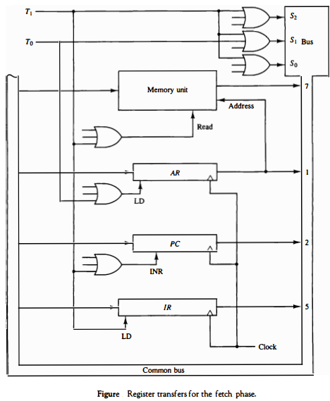
(c) Which are the different phases of Instruction Cycle? Describe Register transfer for fetch phase with its diagram.
The different phases of the Instruction Cycle are:
- Fetch: The fetch phase is the first phase in the instruction cycle. In this phase, the CPU fetches the next instruction from memory whose address is stores in program counter (PC). The PC is incremented to the next instruction after the fetch. The fetched instruction is stored in a special register called the instruction register (IR).
- Decode: In the decode phase, the instruction in the IR is decoded and the necessary operations are identified. Decoding of instruction is basically done with help of opcode.
- Read : Read the effective address from memory if the instruction has an indirect address.
- Execute : In the Execution phase, the instruction is finally executed and the result of the operation is stored back in memory or in a register.
The Instruction cycle continues in loop until the HALT instruction is encountered.
Register Transfer for Fetch Phase:
During the fetch phase, the control unit performs the following register transfer operations:
- The program counter (PC) is loaded with the address of the next instruction to be fetched.
- The contents of the PC are transferred to the memory address register (MAR).
- The control unit sends a read signal to memory, and the contents of the memory location specified by the MAR are transferred to the instruction register (IR).
The diagram of register transfer for fetch phase is as follows:
OR
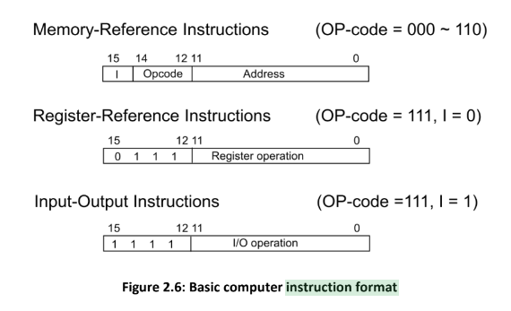
(c) Define: microinstruction; Identify different types of 16 bits instruction formats for basic computer using figure.
A Microinstruction refers to a low-level instruction that defines the operations and control signals necessary to execute a single machine-level instruction. It is used by a microprogrammed control unit to perform operations in a computer’s central processing unit (CPU).
Microinstructions are typically implemented as a sequence of binary values that control various aspects of the processor's behavior, such as fetching data from memory, performing arithmetic or logical operations, and storing results. Each microinstruction corresponds to a specific step in the execution of a machine-level instruction.
Microinstructions are executed internally within the processor and are not directly visible or programmable by software developers.
There are three different types of 16-bit instruction formats for a basic computer:
- Register-reference instructions : These instructions specify a register as an operand and reference it in the operation. They are recognized by the operation code 111 with a 0 in the leftmost bit (bit 15) of the instruction.
- Memory-Reference Instruction uses 12 bits to specify an address and one bit to specify the addressing mode I. I is equal to 0 for direct address and to 1 for indirect address.
- An input-output instruction does not need a reference to memory and is recognized by
the operation code 111 with a 1 in the leftmost bit of the instruction. The remaining 12
bits are used to specify the type of input-output operation or test performed.
Q.3
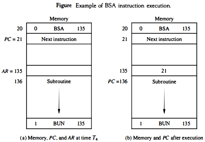
(a) Use BSA and BUN instruction with example and diagram.
- BSA (Branch and Save Return Address) and BUN (Branch Unconditionally) are two types of instructions used in computer programming to change the flow of program execution.
- BSA Instruction: The BSA instruction is used to call a subroutine in a program. It saves the current value of the program counter (the address of the next instruction to be executed) in a register called the Link Register and transfers control to the address specified in the instruction. The Link Register is used to return control to the instruction following the BSA instruction after the subroutine is executed.
- BUN Instruction: The BUN instruction is used to transfer control to a new address unconditionally. It simply sets the program counter to the address specified in the instruction and continues execution from there.
(b) Criticize Three-Address Instructions and Zero address instruction with common example.
Criticisms of Three-Address Instructions:
- They require more memory space to store than other instruction formats, such as one-address or zero-address instructions.
- They can be more complex to decode and execute than other instruction formats.
- They can lead to longer execution times for certain operations that require multiple operands, such as multiplication or division.
Example of Three-Address Instruction: ADD R1, R2, R3 (Adds the values in registers R2 and R3 and stores the result in R1.)
Criticisms of Zero-Address Instructions:
- They can be less flexible than other instruction formats because they only allow operations on the top of the stack.
- They can be slower to execute than other instruction formats because they require more memory access operations to retrieve operands from the stack.
Example of Zero-Address Instruction: POP (Pops the top value from the stack and stores it in a register).
(c) Describe how control unit determine instruction type after the decoding using flowchart for instruction cycle.
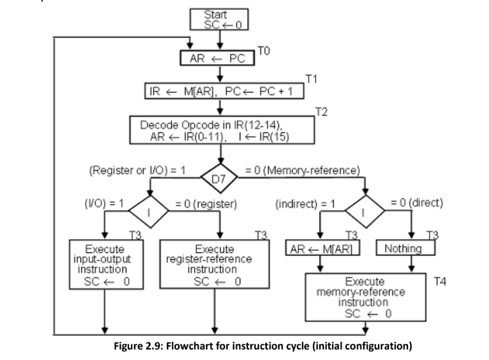
- The flowchart presents an initial configuration for the instruction cycle and shows how the control determines the instruction type after the decoding.
- If D7 = 1, the instruction must be register-reference or input-output type. If D7 = 0, the operation code must be one of the other seven values 110, specifying a memory-reference instruction. Control then inspects the value of the first bit of the instruction, which now available in flip-flop I.
- If D7 = 0 and I = 1, we have a memory-reference instruction with an indirect address. It is then necessary to read the effective address from memory.
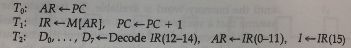
- The three instruction types are subdivided into four separate paths. The selected operation is activated with the clock transition associated with timing signal T3.This can be symbolized as follows: D’7 I T3: AR ←M [AR] D’7 I’ T3: Nothing D7 I’ T3: Execute a register-reference instruction D7 I T3: Execute an input-output instruction
- When a memory-reference instruction with I = 0 is encountered, it is not necessary to do anything since the effective address is already in AR.
- However, the sequence counter SC must be incremented when D’7 I T3 = 1, so that the execution of the memory-reference instruction can be continued with timing variable T4.
- A register-reference or input-output instruction can be executed with the click associated with timing signal T3. After the instruction is executed, SC is cleared to 0 and control returns to the fetch phase with T0 =1. SC is either incremented or cleared to 0 with every positive clock transition.
OR
Q.3
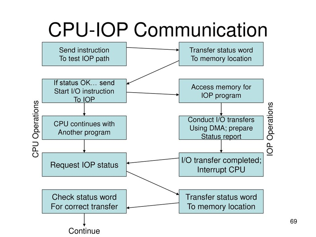
(a) Prepare flowchart of CPU-IOP communication.
(b) Differentiate RISC and CISC architecture. (Use Any Points are per your choice )
| S.No. | RISC | CISC |
|---|---|---|
| 1. | It stands for Reduced Instruction Set Computer. | It stands for Complex Instruction Set Computer. |
| 2. | RISC processors, on the other hand, have a reduced instruction set, which means that each instruction performs a single operation. | CISC processors have a complex instruction set, which means that a single instruction can perform multiple operations |
| 3. | These chips are relatively simple to design. | These chips are complex to design. |
| 4. | RISC processors have more registers compared to CISC processors | CISC processors have less registers compared to RISC processors |
| 5 | RISC processors are designed for pipelining, which means that multiple instructions can be executed simultaneously. | CISC processors are not as efficient for pipelining because of their complex instruction set. |
| 6 | RISC processors rely on compiler optimization to achieve better performance. | CISC processors, on the other hand, rely on hardware to achieve better performance. |
| 7 | RISC processors have a load/store architecture, which means that all operations are performed on registers, and memory access is only allowed through load and store instructions | CISC processors, on the other hand, allow direct memory access. |
| 8. | They are inexpensive. | They are relatively expensive. |
| 9. | Simple addressing formats are supported. | The instructions interact with memory using complex addressing modes. |
| 10. | It doesn't support arrays. | It has a large number of instructions. It supports arrays. |
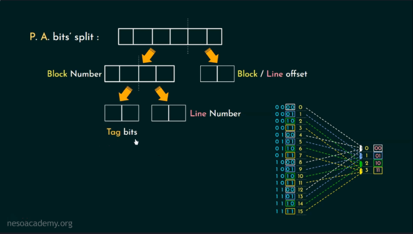
(c) What is cache memory? Interpret direct addressing mapping with diagram.
- Cache memory is a high-speed memory that stores frequently used data or instructions, allowing for faster access than retrieving from the main memory. Direct addressing mapping is a cache mapping technique where each block in the main memory is mapped to exactly one block in the cache memory.
- Main Memory is divided into blocks and Cache memory is divided into lines. Generally the number of blocks in memory are more than the number of lines lines in cache memory, but the size of blocks and line are same.
- No. of blocks = size of main memory / one Block size, for example, In Byte addressable memory : main memory size = 64 words (Byte) , Block size = 4 words (byte), thus no of blocks in main memory would be 16 ( numbered as 0..15 ). Similarly cache memory would also be divided into lines.
- Each Block is exactly mapped to one line in cache memory.
- Physical Address is split into two parts : Block number and Line offset.
Block number is also divided into Tag Bits and Line number.
Tags bits are used to indicate if a particular block is present in cache or not. It yes than it is called cache hit, if not than cache miss.
Line Number is used to indicate that which block would be pointed to which line number.
Line offset is used to determine the particular word inside one line. Ex: line offset of 2 bits can be used to determine 2^2 words inside single line of cache memory.
Q.4
(a) Draw and criticize memory hierarchy in a computer system.
Memory hierarchy is an important aspect of computer architecture that aims to provide a balance between the speed and capacity of memory. The memory hierarchy consists of multiple levels of memory, each with different access times, capacities, and costs.
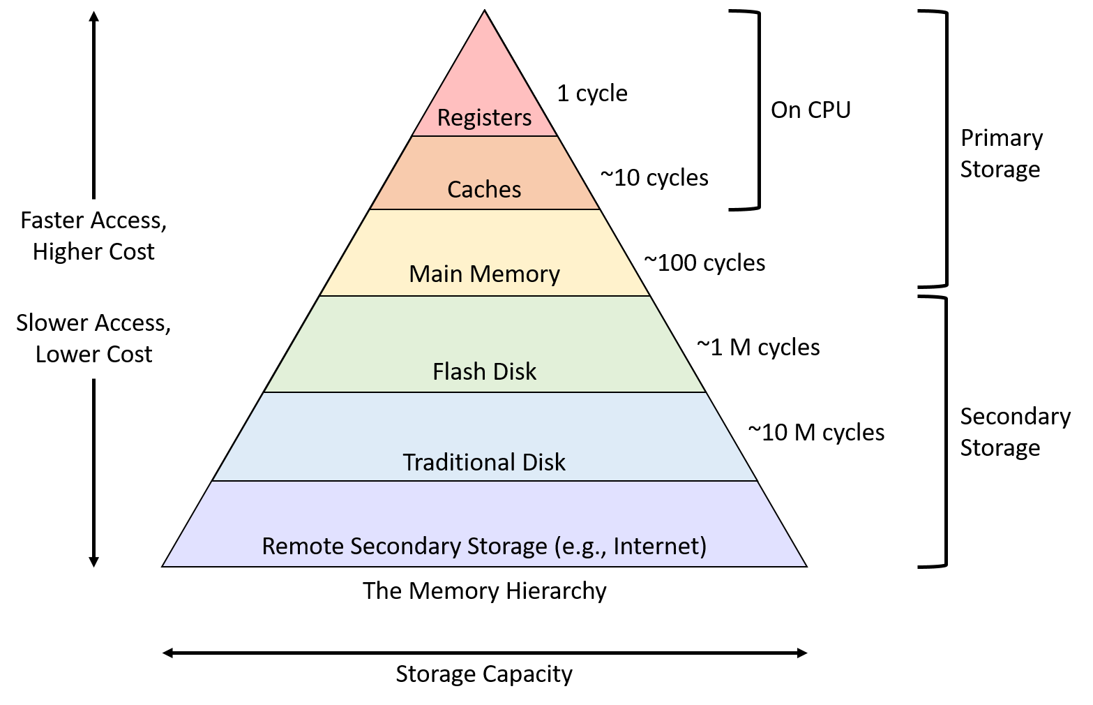
Criticisms of the memory hierarchy include the following:
- Cost: Each level of memory adds cost to the computer system, and designing a memory hierarchy that balances cost and performance can be challenging.
- Complexity: The memory hierarchy adds complexity to the computer system, making it more difficult to design and program.
- Cache coherence: Maintaining cache coherence between multiple processors can be difficult and may require additional hardware and software support.
- Capacity: Each level of memory has a finite capacity, which can lead to cache misses and slower performance.
- Latency: Accessing memory at lower levels of the hierarchy can take longer than accessing higher levels of memory, which can impact performance.
(b) Write an Assembly level program for addition of 50 numbers.
| Memory Address | Mnemonics | RTL | Comment |
|---|---|---|---|
| 2000 | MVI B,50 | B ← 50 | Load the counter with 50 |
| 2002 | LXI H,3000 | H, L ← 3000 | Initialize memory address |
| 2005 | MVI A,0 | A ← 0 | Initialize the accumulator |
| 2007 | ADD M | A ← A + M | Add the number from memory to A |
| 2008 | INX H | - | Increment the memory address |
| 2009 | DCR B | B ← B - 1 | Decrement the counter |
| 200A | JNZ 2007 | Jump to 2007 if NZ | Repeat the loop if B is not zero |
| 200D | HLT | Halt | End of the program |
(c) Draw the flowchart of first pass of the assembler and explain working of the same.
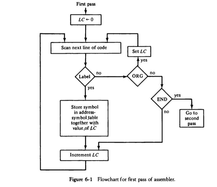
- During the first pass of the assembly process, there are several steps involved. First, a table is created that links user-defined address symbols with their corresponding binary values. Then, in the second pass, the actual translation to binary takes place.
- To keep track of the instructions' memory locations, the assembler uses a memory word called the location counter (LC). This LC holds the value of the memory location currently assigned to the instruction or operand being processed.
- To begin, the assembler sets the LC to 0. Then, each line of code is analyzed. If the line does not have a label (identified by the presence of a comma), the assembler checks the symbol in the instruction field.
- If the instruction field contains an ORG pseudo instruction, the LC is set to the number specified after the ORG, and the assembler moves on to process the next line.
- When an END pseudo instruction is encountered, the first pass terminates, and the assembler proceeds to the second pass.
- If the line of code contains a label, it is stored in the address symbol table along with its corresponding binary value, determined by the current value of LC. If no label is found, nothing is stored in the table.
- After storing the label and updating the table, the LC is incremented by 1, and the process continues with the next line of code. This ensures that instructions are stored in sequential memory locations.
- By following this flowchart and performing these tasks, the assembler successfully completes the first pass of the assembly process.
OR
Q.4
(a) Interpret the following instructions: INP, ISZ and LDA
INP (Input)
The INP instruction is used to read input from an external source, such as a keyboard or a sensor. When the INP instruction is executed, it prompts the system to wait for input from the specified source. Once the input is provided, it is stored in a designated location in memory or a register for further processing by the program.
ISZ (Increment and Skip if Zero)
ISZ is used to increment the contents of a memory location by 1 and then checks whether the result is zero or not. If it is zero, then the program counter is incremented by one, and the next instruction is executed. If it is not zero, the program counter is not changed, and the current instruction is repeated.
LDA (Load Accumulator)
LDA is used to load the contents of a memory location into the accumulator register. When the instruction is executed, the value stored at the specified location is fetched and transferred into the accumulator.
(b) Write an Assembly level program to move one block of data to another location.
| Memory | Mnemonics | Operands | Comment |
|---|---|---|---|
| 2000 | MVI | C, 05 | [C] ← 05 |
| 2002 | LXI | H, 2500 | [H-L] ← 2500 |
| 2005 | LXI | D, 2600 | [D-E] ← 2600 |
| 2008 | MOV | A, M | [A] ← [[H-L]] |
| 2009 | STAX | D | [A] → [[D-E]] |
| 200A | INX | H | [H-L] ← [H-L] + 1 |
| 200B | INX | D | [D-E] ← [D-E] + 1 |
| 200C | DCR | C | [C] ← [C] – 1 |
| 200D | JNZ | 2008 | Jump if not zero to 2008 |
| 2010 | HLT | Stop |
Explanation – Registers A, D, E, H, L, C are used for general purpose:
- MOV is used to transfer the data from memory to accumulator (1 Byte)
- LXI is used to load register pair immediately using 16-bit address (3 Byte instruction)
- MVI is used to move data immediately into any of registers (2 Byte)
- STAX is used to store accumulator into register pair indirectly (3 Byte instruction)
- DCR is used to decrease register by 1 (1 Byte instruction)
- INX is used to increase register pair by 1 (1 Byte instruction)
- JNZ is used to jump if not zero to given memory location (3 Byte instruction)
- HLT is used to halt the program
(c) List out modes of transfer. Formulate direct memory access technique in detail.
We store the binary information received through an external device in the memory unit. The information transferred from the CPU to external devices originates from the memory unit. Although the CPU processes the data, the target and source are always the memory unit. We can transfer this information using three different modes of transfer
- Programmed I/O
- Interrupt-driven I/O
- Direct Memory Access (DMA)
Direct Memory Access (DMA) is a technique used to transfer data directly between I/O devices and memory without involving the CPU. This technique is used to reduce the CPU’s workload and increase the overall system performance.
This technique is used in situations where a large amount of data needs to be transferred between memory and an I/O device. It allows the CPU to perform other tasks while the data transfer is taking place, thus increasing system performance.
The steps involved in the DMA transfer are as follows:
- The CPU sets up the DMA controller (DMAC) with the transfer parameters, including the starting memory address, the device address, and the number of bytes to transfer.
- The DMA controller requests control of the system bus from the CPU using BUS REQUEST.
- The CPU releases the bus to the DMA controller (BUS GRANT) , which then reads or writes data directly to or from memory and I/O devices.
- Once the transfer is complete, the DMA controller returns control of the system bus to the CPU.
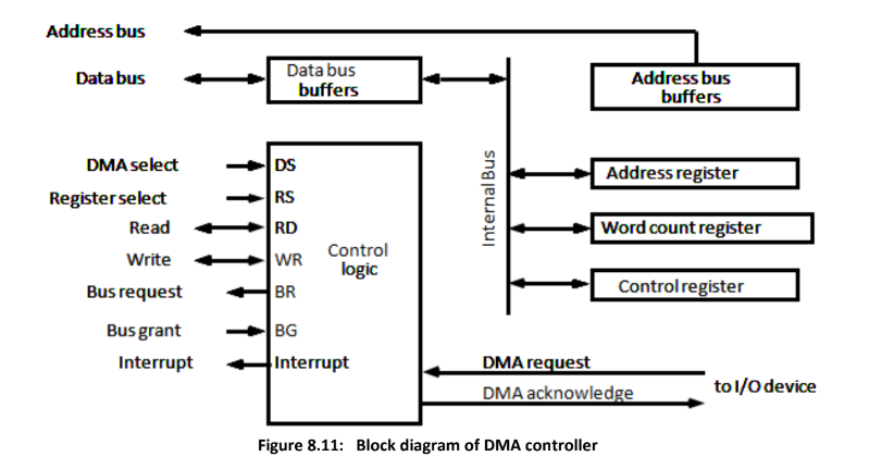
DMA Controller :
Facilitates communication between the CPU, I/O device, and memory.
It requires an address register, word count register, and address lines.
The address register and lines are used for direct communication with memory. The word count register specifies the number of words to be transferred..
CPU selects DMA registers using the address bus and DS/RS inputs.
RD and WR inputs allow bidirectional communication.
When BG is 0, the CPU can access DMA registers through the data bus. When BG is 1, DMA can communicate directly with memory using the address bus and RD/WR control.
DMA communicates with peripherals through request and acknowledge lines.
Q.5
(a) Summarize major hazards in pipelined execution.
Pipelining is a technique used in computer processors to improve performance by breaking down instructions into smaller steps that can be executed in parallel. However, pipelining can lead to hazards that can slow down the execution of instructions.
The major hazards in pipelined execution are:
- Structural hazards : arise when multiple instructions require the same hardware resource simultaneously. This can be resolved by adding more hardware or rearranging pipeline stages.
- Data hazards : occur when an instruction depends on the results of a previous instruction that is still being processed in the pipeline. This can be resolved by forwarding data or stalling the pipeline until the data is available.
- Control hazards : arise when the pipeline needs to make decisions based on conditional instructions before their results are available. This can be resolved using branch prediction techniques or delaying the execution of conditional instructions until the results are ready
By identifying and resolving these hazards, pipelined execution can be optimized for high performance.
(b) What is a data dependency conflict in instruction pipeline? Recommend solutions for data dependency conflicts.
In instruction pipeline, data dependency conflict occurs when an instruction depends on data produced by a previous instruction that has not yet completed its execution in the pipeline. This dependency creates a conflict as the pipeline cannot move forward until the data is available, leading to pipeline stalls and reduced performance.
There are several solutions to data dependency conflicts in instruction pipelines:
- Forwarding or data forwarding: This technique involves bypassing the intermediate stages of the pipeline and directly forwarding the data from the output of the earlier stage to the input of the later stage that needs it. This solution reduces pipeline stalls and improves performance.
- Stalling or pipeline flushing: This technique involves stopping the pipeline until the required data is available. This solution eliminates the possibility of data hazards but can reduce performance.
- Register renaming: This technique involves duplicating registers to eliminate the dependency between instructions and avoid data hazards. This solution reduces pipeline stalls and improves performance.
- Speculative execution: This technique involves executing instructions speculatively based on the assumption that the data dependency will not occur. If the assumption is incorrect, the pipeline is flushed, and the instructions are re-executed. This solution can improve performance but requires additional hardware support.
- Compiler optimization: This technique involves restructuring the code to reduce data dependencies and improve pipeline performance. This solution requires changes to the code and may not always be feasible.
Overall, the choice of solution depends on the design goals and constraints of the pipeline. A combination of these solutions may be used to optimize pipeline performance.
(c) Demonstrate four-segment instruction pipeline in detail.
- A four-segment instruction pipeline combines two or more different segments and makes it as a single one.
- For Example, Assume that the decoding of the instruction can be combined with the calculation of the effective address into one segment. Assume further that most of the instructions place the result into a processor registers so that the instruction execution and storing of the result can be combined into one segment.
- This reduces the instruction pipeline into four segments.
- FI: Fetch an instruction from memory
- DA: Decode the instruction and calculate the effective address of the operand
- FO: Fetch the operand
- EX: Execute the operation
- Flowchart showing how the instruction cycle in the CPU can be processed with a four segment pipeline
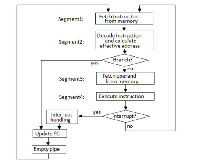
- Each segment represents a different stage of instruction processing. While one instruction is being executed, the next instruction is fetching an operand from memory.
- The effective address can be calculated separately for one instruction, allowing subsequent instructions to be fetched and placed in an instruction FIFO. This enables up to four sub-operations to overlap, allowing four different instructions to be processed simultaneously.
- For Example refer this figure for the operation of the pipeline :
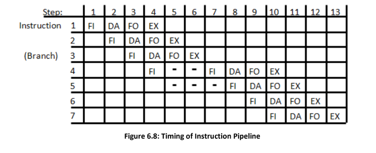
- In step 4, instruction 1 is executed, instruction 2 fetches an operand, instruction 3 is decoded, and instruction 4 is fetched from memory. If a branch instruction (instruction 3) is encountered, the transfer of other instructions is halted until the branch instruction is executed in step 6.
- Depending on the branch outcome, a new instruction may be fetched in step 7 or the previously fetched instruction is used. Delays may occur if the EX segment needs to store a result while the FO segment fetches an operand, requiring FO to wait until EX completes its operation.
OR
Q.5
(a) Sketch Microinstruction code format. Quote BR and CD field in brief.
- A microinstruction format includes 20 bits in total. They are divided into four elements as displayed in the figure:
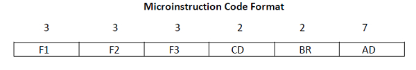 F1, F2, F3 are the micro-operation fields. They determine micro-operations for the computer.
CD is the condition for branching. They choose the status bit conditions.
BR is the branch field. It determines the type of branch.
AD is the address field. It includes the address field whose length is 7 bits.
F1, F2, F3 are the micro-operation fields. They determine micro-operations for the computer.
CD is the condition for branching. They choose the status bit conditions.
BR is the branch field. It determines the type of branch.
AD is the address field. It includes the address field whose length is 7 bits. - The combination of F1,F2,F3 binary (3 bit each) can determine various micro-operations. Refer Table online.
BR (Branch)
The BR (branch) field includes 2 bits. It can be used by connecting with the AD (address) field. The reason for connecting with the AD field is to select the address for the next microinstruction. The table illustrates the various branch fields and their functions. (optional)
| BR | Symbol | Comments |
|---|---|---|
| 00 | JMP | CAR ←AD if condition = 1 |
| CAR←CAR + 1 if condition = 0 | ||
| 01 | CALL | CAR ←AD , SBR ← CAR +1, if condition = 1 |
| CAR←CAR + 1 if condition = 0 | ||
| 10 | RET | CAR ←SBR (Return from subroutine) |
| 11 | MAP | CAR(2-5) ←DR(11-14), CAR(0,1,6) ←0 |
CD (Condition)
A condition field includes 2 bits. They are encoded to define four status bit conditions.
Table (optional)
| CD | Condition | Symbol | Comments |
|---|---|---|---|
| 00 | Always = 1 | U | Unconditional Branch |
| 01 | DR (15) | I | Indirect address bit |
| 10 | AC (15) | S | Sign bit of AC |
| 11 | AC = 0 | Z | Zero value in AC |
**(b) Compare following terms:
Write throughs-cache and Write back cache. Spatial locality and Temporal locality. **
| Aspect | Write-Through Cache | Write-Back Cache |
|---|---|---|
| Write Operation Performance | Lower write performance compared to write-back cache | Higher write performance compared to write-through cache |
| Read Operation Performance | Lower read performance compared to write-back cache | Higher read performance compared to write-through cache |
| Implementation Complexity | Easier to implement as it doesn't require handling evictions and writebacks | More complex implementation due to the need for eviction and writeback handling |
| Data Consistency | Less prone to data inconsistencies if properly implemented | More prone to data inconsistencies if not properly implemented |
- Write-through cache and write-back cache:
- Write-through and write-back are two techniques used in computer caches to manage data updates.
- In a write-through cache, every write to the cache is immediately written to the main memory as well.
- In a write-back cache, data is only written back to the main memory when it is evicted from the cache.
Spatial locality and temporal locality: Spatial locality and temporal locality are two principles that describe how data is accessed in computer systems.
Spatial locality refers to the tendency of a program to access data that is located near other recently accessed data. For example, when accessing an array, the program is likely to access the adjacent elements as well, due to the way arrays are stored in memory.

Temporal locality refers to the tendency of a program to access the same data repeatedly over a short period. For example, a loop that repeatedly processes a large array will exhibit high temporal locality, as the same data is accessed multiple times.
Aspect Spatial Locality Temporal Locality Definition Refers to accessing data located near other recently accessed data Refers to repeated access to the same data over a short period Importance for Cache Important for cache performance as it allows caching of nearby data to reduce latency Important for cache performance as it allows caching of frequently accessed data to reduce latency Impact on Memory Access Latency Reduces memory access latency by utilizing cached nearby data Reduces memory access latency by utilizing cached frequently accessed data Relation to Data Structures Related to how arrays are stored in memory, accessing adjacent elements Related to repeated access in loops or within a short period Importance for System Important for optimizing cache performance and reducing memory access latency Important for optimizing cache performance and reducing memory access latency Overall Significance Key principle for designing efficient caching and memory systems Key principle for designing efficient caching and memory systems Overall, spatial and temporal locality are both important principles for optimizing computer system performance, and understanding them can help in designing more efficient caching and memory systems ### **(c) Elaborate Flynn’s classification scheme with proper diagram.** - Flynn’s classification scheme is a taxonomy that categorizes computer architectures based on the number of instruction streams and data streams that can be processed simultaneously. The scheme was introduced by Michael J. Flynn in 1966 and is still widely used in computer science. - The Flynn’s classification scheme divides computer architectures into four categories based on two dimensions: instruction stream and data stream. The instruction stream dimension indicates the number of concurrent instruction streams, while the data stream dimension indicates the number of concurrent data streams.  - Here are the four categories of computer architectures in Flynn’s classification scheme: 1. SISD (Single Instruction Stream, Single Data Stream): This is the traditional type of computer architecture, in which a single instruction stream controls the flow of operations, and a single data stream provides the operands for the instructions. This type of architecture is used in most traditional von Neumann computers. 2. SIMD (Single Instruction Stream, Multiple Data Stream): In this architecture, a single instruction stream is used to perform the same operation on multiple data streams simultaneously. SIMD computers are optimized for tasks that can be performed using parallelism, such as graphics processing and scientific simulations. 3. MISD (Multiple Instruction Stream, Single Data Stream): In this architecture, multiple instruction streams are executed on a single data stream. MISD computers are not commonly used in practice, but they can be used in safety-critical systems, such as aerospace or nuclear power plants, where multiple redundant processors can check each other’s results. 4. MIMD (Multiple Instruction Stream, Multiple Data Stream): This architecture allows for multiple instruction streams and data streams to be processed simultaneously, providing the highest level of parallelism. MIMD computers can be further divided into two subcategories: shared-memory and distributed-memory architectures. In shared-memory MIMD computers, all processors share a common memory, while in distributed-memory MIMD computers, each processor has its own local memory and communicates with other processors via a communication network. - Flynn’s classification scheme provides a useful framework for understanding the capabilities and limitations of different computer architectures. By categorizing architectures based on their ability to handle instruction and data streams, it helps to identify which architectures are best suited for different types of applications.